Psalm 37:4–5 (KJV)
4 Delight thyself also in the LORD; and he shall give thee the desires of thine heart.
5 Commit thy way unto the LORD; trust also in him; and he shall bring it to pass.
Watch the Complete Video:
In the video, we explain the NAND gate truth table, build the SR latch, demonstrate the LED, and examine the circuit using our DSO138 oscilloscope.
How to Eliminate Switch Bounce Using NAND Gates! | SN7400N
Have you ever flipped a mechanical switch and wondered why your electronic circuit sometimes detects several signals instead of just one?
The culprit may be mechanical switch bounce!
In this experiment, we’ll use the SN7400N quad 2-input NAND gate IC to build a simple SR latch that eliminates unwanted switch-bounce transitions at the output.
We’ll also use our DSO138 oscilloscope to examine the raw mechanical switch signal and observe the clean output from our NAND gate latch.
What Is Mechanical Switch Bounce?
When you operate a mechanical switch, its metal contacts don’t always settle immediately.
Instead, they may briefly make and break their electrical connection several times before coming to rest.
These rapid changes can cause digital circuits to interpret a single switch operation as multiple events.
For example, a digital counter might count several pulses even though you only operated the switch once.
In our previous video, we examined mechanical switch bounce using the DSO138 oscilloscope.
Now we’re going to solve that problem!
Meet the SN7400N NAND Gate IC
The SN7400N contains four independent 2-input NAND gates in a 14-pin DIP package.
A NAND gate produces a LOW output only when both inputs are HIGH.
NAND Gate Truth Table
-
A = 0, B = 0 → Output = 1
-
A = 0, B = 1 → Output = 1
-
A = 1, B = 0 → Output = 1
-
A = 1, B = 1 → Output = 0
Remember: A NAND gate produces a LOW output only when both inputs are HIGH.
For our experiment, we’re using two of the four NAND gates.
-
Gate 1: Inputs on pins 1 and 2, output on pin 3.
-
Gate 2: Inputs on pins 4 and 5, output on pin 6.
-
Pin 14: +5 V supply.
-
Pin 7: Ground.
Building an SR Latch
An SR latch is a simple digital circuit that can remember one of two states.
We’ll construct ours using two cross-coupled NAND gates.
The feedback connections are:
-
Pin 3 connects to pin 5.
-
Pin 6 connects to pin 2.
These connections allow the two gates to maintain their output states after the switch changes position.
Our SPDT slide switch has its common terminal connected to ground.
One contact connects to pin 1, while the other connects to pin 4.
Two 10 kΩ pull-up resistors keep these inputs HIGH whenever they’re not connected to ground.
When the switch moves to contact A, pin 4 is pulled LOW and pin 6 goes HIGH.
When the switch moves to contact B, pin 1 is pulled LOW and pin 6 goes LOW.
During the brief interval when neither contact is connected, both inputs are HIGH, allowing the latch to retain its previous state.
That’s the key to eliminating switch bounce!
Circuit Diagram:
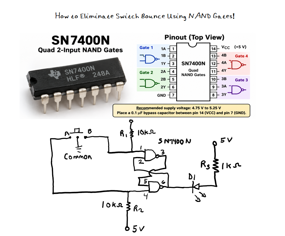
Our circuit includes an LED indicator connected to pin 6 through a 1 kΩ current-limiting resistor.
The LED is connected to the positive supply, so it turns ON when pin 6 is LOW and turns OFF when pin 6 is HIGH.
We also connect the unused NAND gate inputs (pins 9, 10, 12, and 13) HIGH through a shared 2.2 kΩ resistor. The unused outputs (pins 8 and 11) remain unconnected.
A 0.1 µF ceramic bypass capacitor is connected between pins 14 and 7, close to the IC.
Components Used
Want to build this circuit yourself? Here are the components and equipment used in this experiment.
Affiliate Disclosure: As an Amazon Associate, I earn from qualifying purchases. The Amazon product links below are affiliate links. If you purchase through these links, I may earn a commission at no additional cost to you.
-
SN7400N Quad 2-Input NAND Gate IC
https://link.amazon/B032rpPJM -
SPDT Slide Switch
https://link.amazon/B09guna18 -
Two 10 kΩ Pull-Up Resistors
https://link.amazon/B03XFnNUj -
2.2 kΩ Resistor for Unused Inputs
https://link.amazon/B03XFnNUj -
1 kΩ LED Current-Limiting Resistor
https://link.amazon/B03XFnNUj -
0.1 µF Ceramic Bypass Capacitor
https://link.amazon/B00l9i6kJ -
Breadboard and Jumper Wires
https://link.amazon/B0gQDnGBQ -
Regulated 5 V DC Power Supply
https://link.amazon/B06BdDrfX -
DSO138 Oscilloscope
https://link.amazon/B0baLTxQj
Testing the Circuit With an LED
We first tested our circuit using the LED indicator.
With the switch in position B, pin 6 was LOW and the LED turned ON.
Moving the switch to position A caused pin 6 to go HIGH and the LED turned OFF.
The LED confirmed that our latch was responding to the switch, but the transitions happened too quickly to evaluate switch bounce visually.
For that, we needed our oscilloscope!
Examining the Raw Switch Input
We connected our DSO138 oscilloscope probe to pin 4, with the ground lead connected to circuit ground.
Our oscilloscope settings were:
-
Time base: 50 µs/div
-
Vertical scale: 1 V/div
-
Coupling: DC
With the switch initially in position B, pin 4 was HIGH.
Moving the switch to position A caused the raw input to transition from HIGH to LOW.
Mechanical contact bounce can produce several rapid transitions during this operation.

Examining the Debounced Output
Next, we moved our single oscilloscope probe to pin 6, the output of our NAND gate latch.
We returned the switch to position B and then moved it to position A.
This produced a LOW-to-HIGH rising edge at pin 6.
Unlike the raw mechanical switch signal, the latch output produced a clean transition without repeated bounce pulses.
The two measurements were captured separately using the same oscilloscope probe.

Why Does the SR Latch Eliminate Bounce?
The secret is the feedback between the NAND gates.
When the SPDT switch moves away from one contact, both latch inputs are temporarily HIGH.
Instead of changing state, the latch remembers its previous state.
When the switch reaches the opposite contact, the latch changes state.
If that contact bounces, the latch retains its new state.
This prevents repeated mechanical contact transitions from producing repeated changes at the output under normal break-before-make switching conditions.
It’s a simple but effective digital solution!
SN7400 Datasheet (Texas Instruments)
For more information about the SN7400N, including its electrical characteristics, pin assignments, and recommendations for unused inputs, visit the official Texas Instruments datasheet:
https://www.ti.com/lit/ds/symlink/sn7400.pdf
Final Thoughts
Mechanical switch bounce is a common problem in digital electronics.
Fortunately, we can solve it using just two NAND gates and a few basic components.
By connecting the gates as an SR latch, we create a circuit that remembers its state and produces clean output transitions.
This is a great example of how digital logic can solve a practical electronics problem.
I hope you enjoyed this experiment and learned something useful along the way!
Thanks for visiting Build Circuits With Rich, and be sure to check out my other hands-on electronics projects!
Want more electronics lessons?
For more beginner-friendly electronics lessons, circuit walkthroughs, and hands-on breadboard builds, visit:
https://buildcircuitswithrich.com
Prefer video?
Watch full lessons on the Build Circuits With Rich YouTube Channel.
Back To: Videos